Multi layer printed circuit board
Overview
By electrically connecting each layer with a through-hole, it becomes a printed wiring board with high reliability.
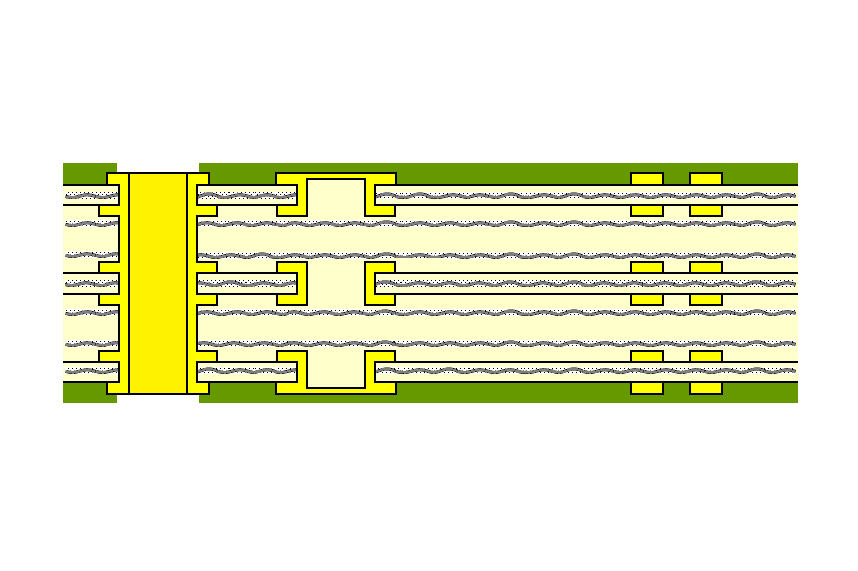
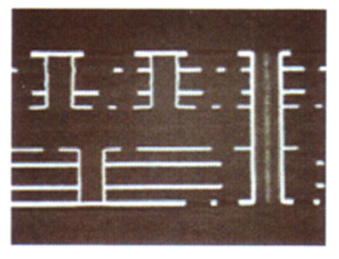
Through-hole structure
16 layers Through-hole connection
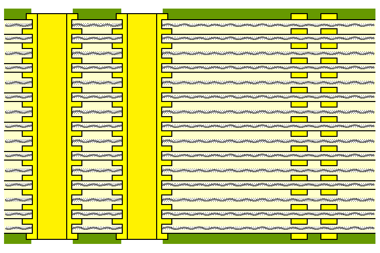
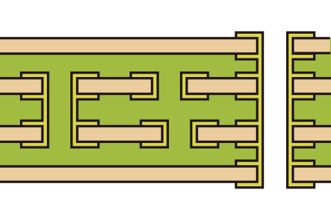
SVH structure
8 layer board SVH
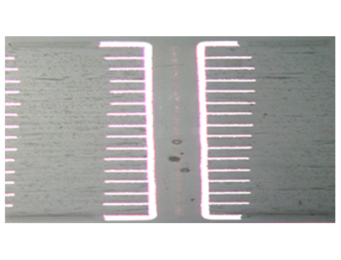
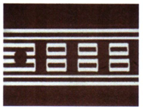
IVH structure
8 layer board SVH
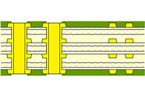
Thick copper specification
- Features
-
Through-hole structure
High-reliability is ensured because the high-multilayer structure is connected by a through-hole.
SVH structure
Component mounting becomes possible right above the through hole, making it possible to reduce the board size.
IVH structure
Since it connects only inside the board with a through hole, miniaturization of board size and high density wiring become possible
- Use
-
AV equipment · home appliances
amusement
Industrial equipment · Lighting
Car audio / navigation
Onboard (ECU, body, electric power steering etc.)
Standard specification
| Items | Standard specification | ||
|---|---|---|---|
| External layer | Min. Conductor width | 0.1mm(0.075) | |
| Min. Spacing of conductor | 0.1mm(0.075) | ||
| Internal layer | Min. Conductor width | 0.1mm | |
| Min. Spacing of conductor | 0.1mm | ||
| Conductor thickness of external layer | 18µm(35) | ||
| Conductor thickness of internal layer | 35µm(18) | ||
| Plating thickness of through hole (Combination Type) | IVH | 15µm | |
| TH | 15µm | ||
| Via | Smallest land diameter of external layer | Bump | φ0.4mm |
| TH | φ0.5mm | ||
| Smallest land diameter of internal layer | Bump | φ0.4mm | |
| TH | φ0.5mm | ||
| Smallest hole diameter | IVH | φ0.2mm | |
| TH | φ0.25mm | ||
| Number of layer | 4,6,8 | ||