Laser build-up printed circuit board
Overview
With the laser build-up structure, it becomes a printed wiring board that can be thinned and downsized.
Laser build-up type
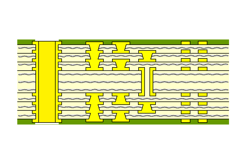
Stacker via structure
LVH 2-stage stacker connection
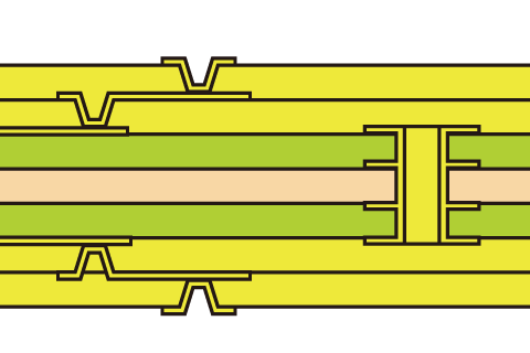
Stack via structure
5 steps just above the IVH
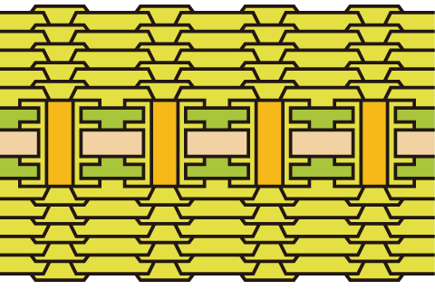
10-stage coreless connection
All-stage prepreg composition
- Features
-
It is possible to cope with thinning and miniaturization by wiring board using correlation connection technology by laser via.
With high density wiring, narrow pitch CSP can be mounted.
- Use
-
AV equipment · home appliances
amusement
Health · Medical
Industrial equipment · Lighting
On-board
- Stack-up
-
Multilayer
HDI
- Number of layers
-
4 layers and 6layers
Standard specification
| Items | Standard specification | ||
|---|---|---|---|
| External layer | Min. Conductor width | 0.075mm | |
| Min. Spacing of conductor | 0.075mm | ||
| Internal layer | Min. Conductor width | 0.1mm(0.075) | |
| Min. Spacing of conductor | 0.1mm(0.075) | ||
| Conductor thickness of external layer | 18µm | ||
| Plating thickness of through hole (Combination Type) | IVH | 15µm | |
| TH | 20µm | ||
| Via | Smallest land diameter of external layer | Laser-via | φ0.275(φ0.25) |
| TH | φ0.6 | ||
| Smallest land diameter of internal layer | Laser | φ0.275(φ0.25) | |
| TH | φ0.5 | ||
| Smallest hole diameter | IVH | φ0.2 | |
| TH | φ0.25 | ||
| Number of layer | 4. 6. 8, 10 | ||